
When creating a PCB layout in KiCad, I often have need to add a mechanical part to the PCB layout. The easy way is to add these parts directly from within PCB New. The problem is that when updating the board from the schematic, it is possible that these extra footprints will be removed. In this post I describe my workaround as well as how I use KiCad’s 3D view to verify these mechanical parts. In addition I describe my approach to managing those symbols and footprints that I tend to use often.
Configuring shared libraries
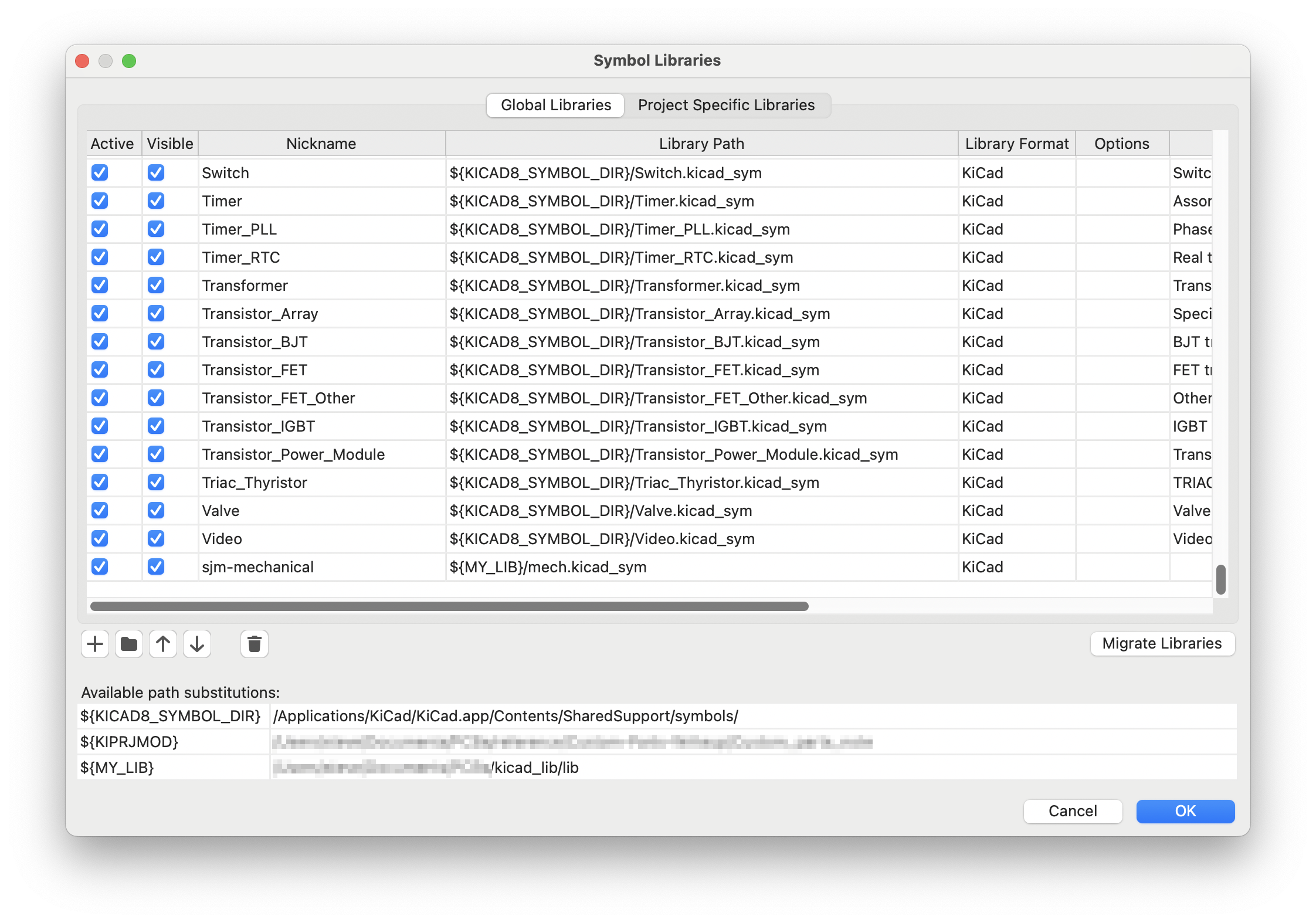
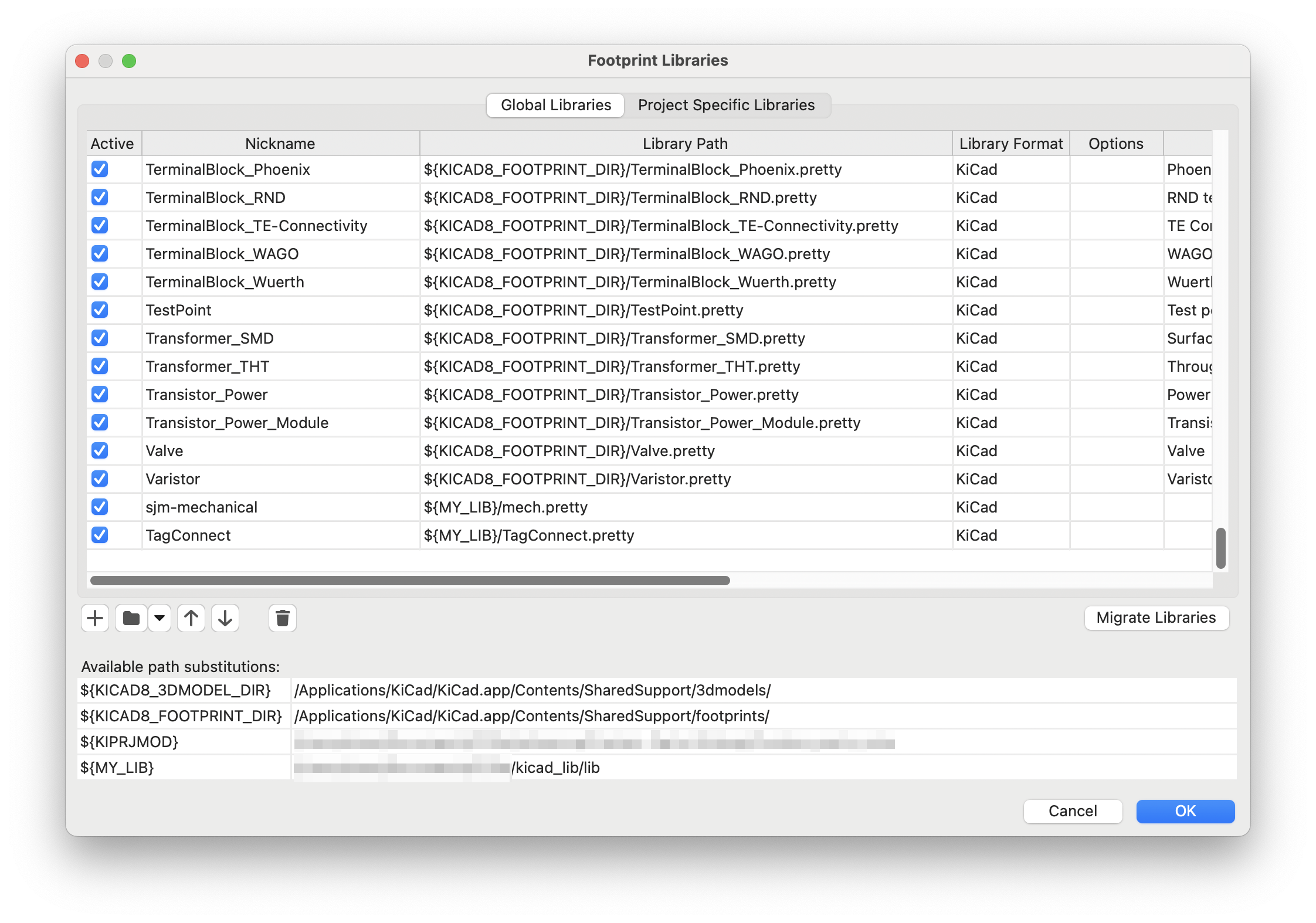
KiCad provides a comprehensive means to manage libraries of symbols and footprints. They are easy to create for each project but there are times when I need to reuse a symbol or footprint from another project. I have sifted through previous projects looking for these parts enough times to realise I needed to do something about it – and make use of the global symbol and footprint configurations.
I also go between a laptop and a PC in the lab so the first thing is to set up some paths so that the artefacts can be seamlessly located between machines. Once KiCad is opened, go to the Preferences, Configure Paths… menu options. I created an environment variable called MY_LIB and pointed this to a repository where I keep all the symbols and footprints I wish to share. As long as I refer to the symbols and footprints via ${MY_LIB}, it does not matter where they are stored on the respective machine. I only needed to perform this operation once per machine.
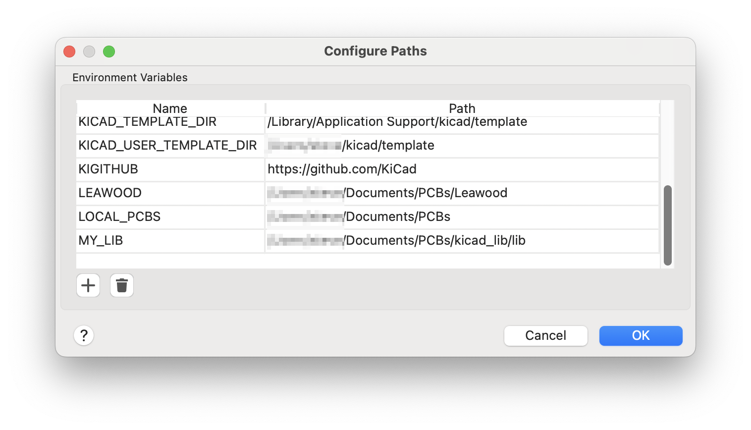
Once the path variable is setup, I can then define the shared libraries I require in the global libraries sections. Here I created them as sjm-mechanical. A future task will be to organise my shared parts repository better.
Creating the symbol
To protect an element from removal, I use the basic workflow of creating a symbol for the mechanical part first and then associating the footprint to that symbol. This way whenever the layout is updated from the schematic, the mechanical elements of the design will always remain in place. It is possible to lock a footprint on the layout. However I personally find this approach tedious and can still result in vanishing elements when I forget to lock it again after I have moved it.
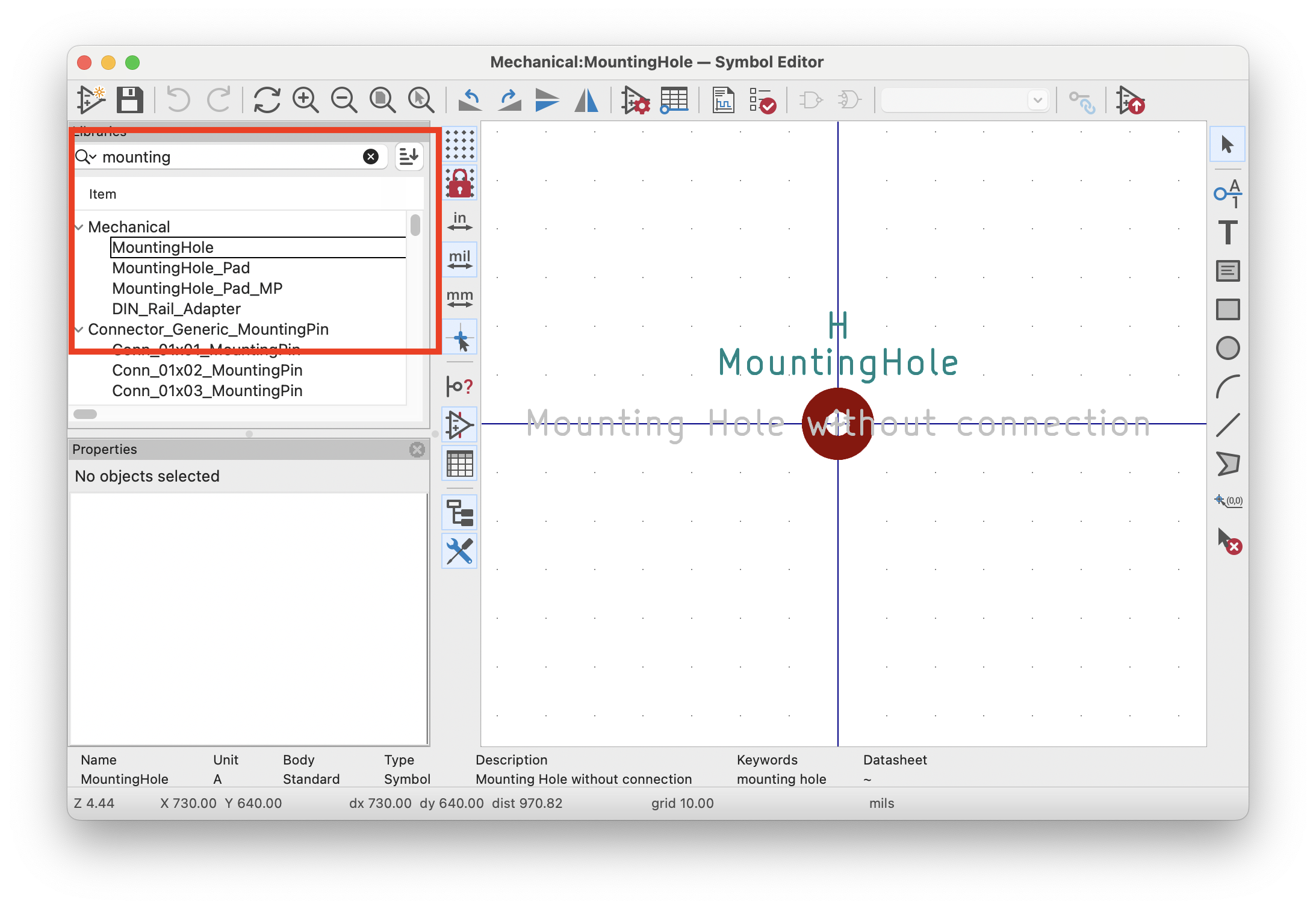
To save a bit of time, it is a good idea to check if there is a symbol already available first before creating a new one. If the symbol can’t be found or it does not suit my purpose, then it is possible to be creative and create something suitable. Another tip would be to make a quick check on the internet to see if there isn’t already a standard symbol for such an element. Below are some of the elements I have used or created.
 | A place holder for a mounting hole. A symbol is needed for each mounting hole to be modelled on the board. |
| Like the mounting hole, for each logo or image to be displayed on the board, a seperate symbol is required. | |
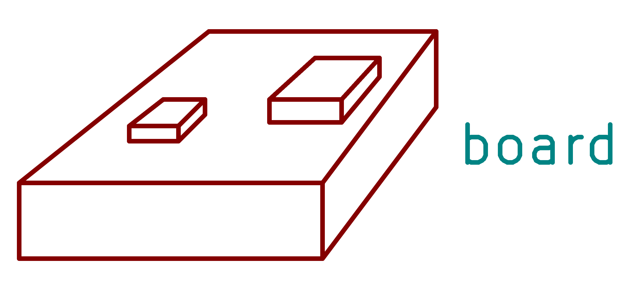 | The board reference is used to define some other mechanical component to be included in the model. This is really only of use in the 3D view where the board under design should be plugged into some other board or vice versa. |
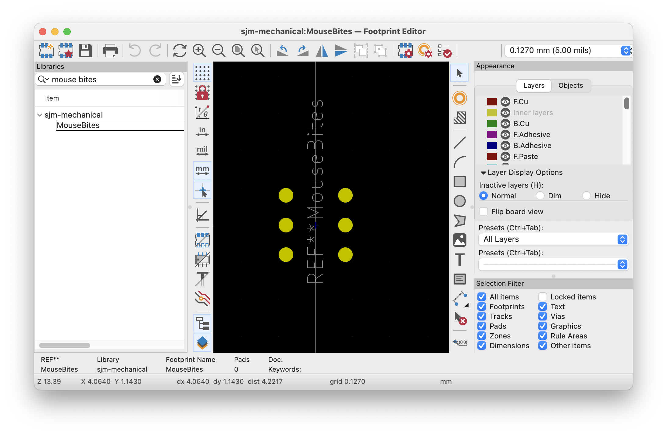
 | Mouse bites are those perforations added between two boards such that they can be easily separated after fabrication. |
Defining the footprint
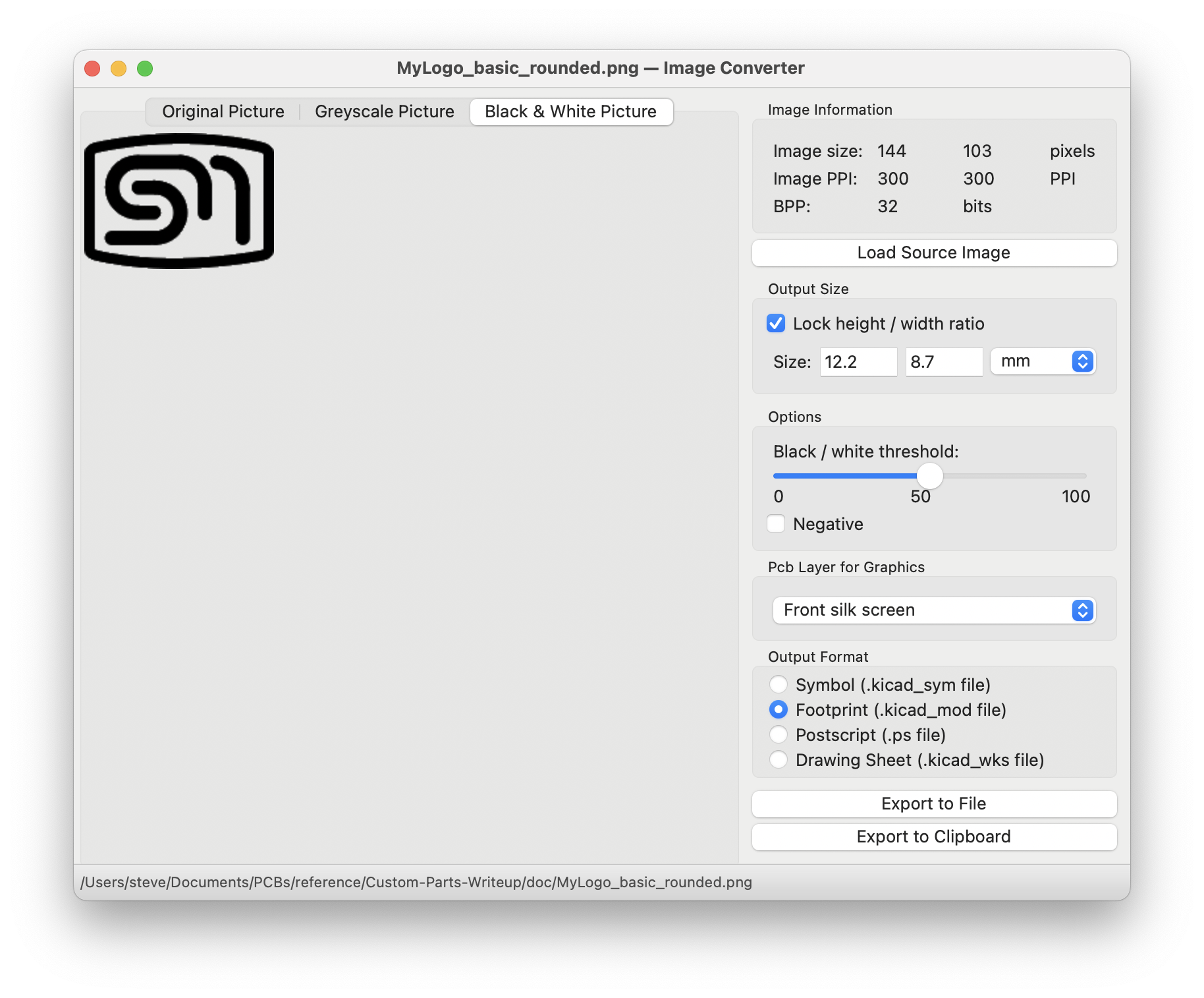
Generally, defining the footprint follows the same procedure as any other footprint. If the footprint is already given amongst the default footprints such as the mounting holes, then I use those. Logos are imported via the Image Converter that will convert a bit image to a KiCad formatted component such as a foot print for use in the PCB layout tool. In the Image Converter, it is possible to select which layer the element should appear on. Here you have the opportunity to create a logo or image that should be on the silk screen layer or to copper layer to create other logo/image effects.
In the case of the mouse bites element, I could not find anything suitable so I created my own.
Associating 3D models
I often use the 3D model view to verify the mechanical aspects of the design checking for the following
- Labels and text hidden by components that are off-board.
- The aesthetic position of labels and text.
- Ensuring that the board being designed will match the external board it is to interface to.
Since many of these symbols represent mechanical or artwork elements, they don’t require any 3D models. The board reference is a special case. When I am creating a board that will accept another board or is to plug into some 3rd party module, then I like to use the 3D view to verify this aspect of the design.
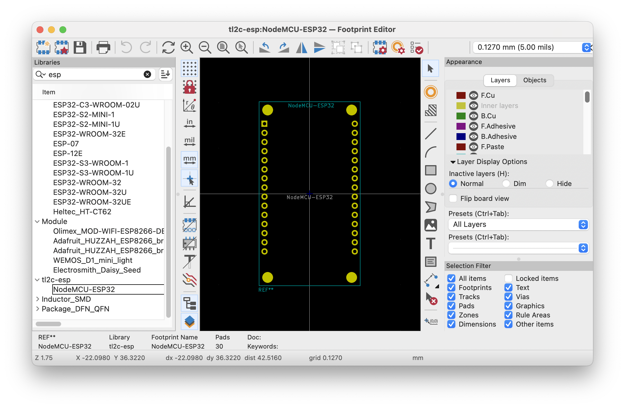
In this example, I created the footprint as normal to model the pin headers for the NodeMCU ESP-32. I then source a 3D model of the 3rd party board in question. One source I use is GrabCad. If I can’t locate what I am looking for then I will use FreeCAD to create my own.
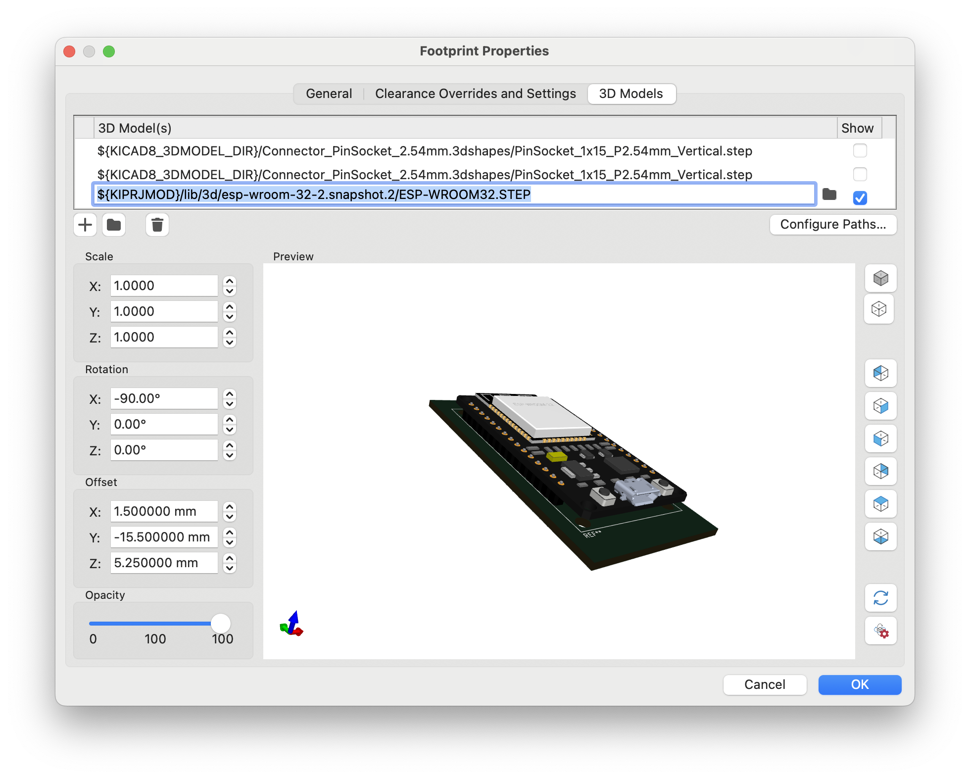
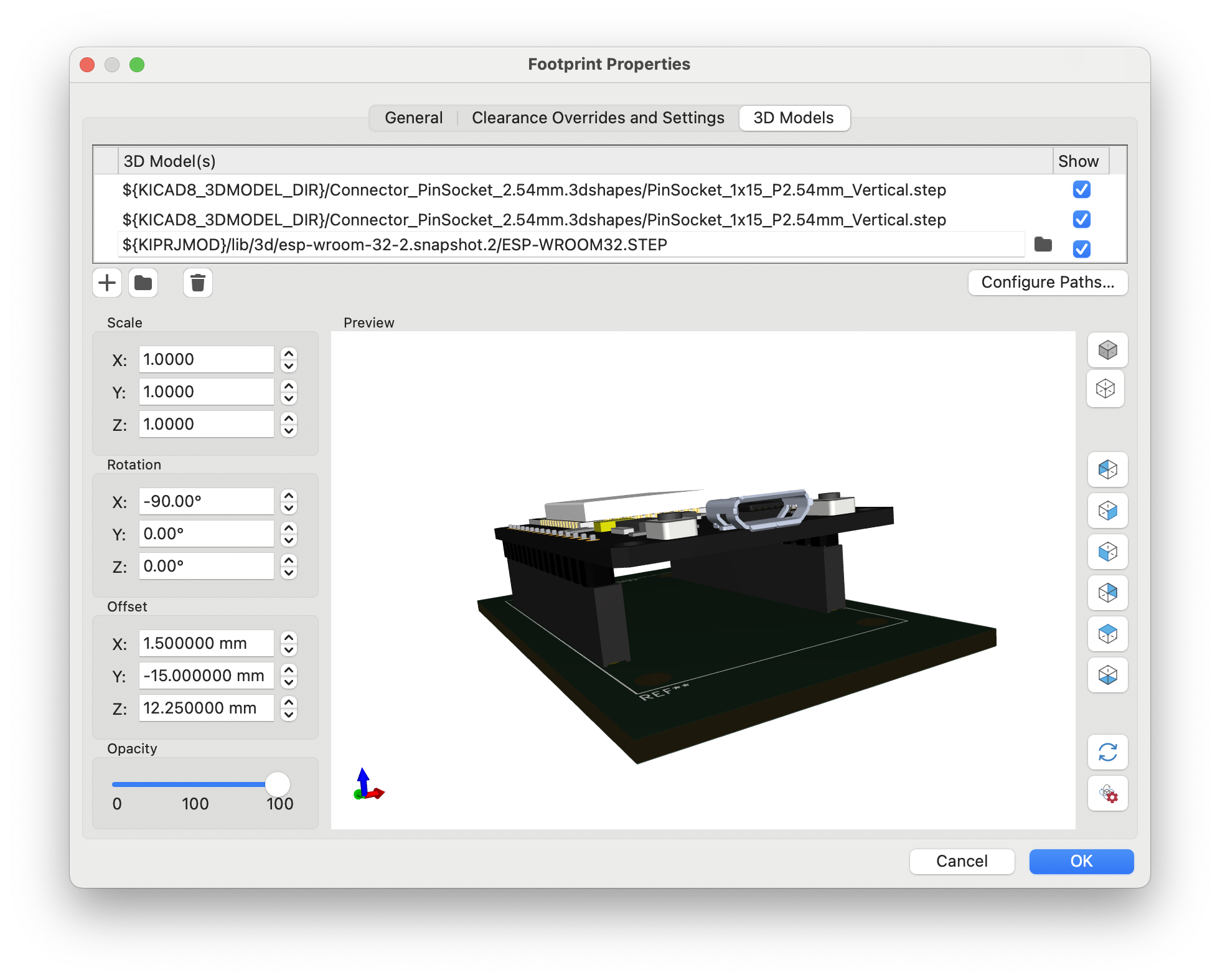
The next step is to associate the 3D model with the footprint using the Footprint Properties tab  . Check the files stored at the directory pointed to by ${KICAD8_3DMODEL} for something suitable e.g. pin headers etc. It is usual then to set the Scale, Rotation and or offset to position the 3D model to the desired position on the footprint displayed on the board. KiCad allows you to define multiple 3D models. They can be selected or deselected for display as required. In this example, I used this technique to explore what it would be like to use pin headers rather than soldering the NodeMCU board directly to my project.
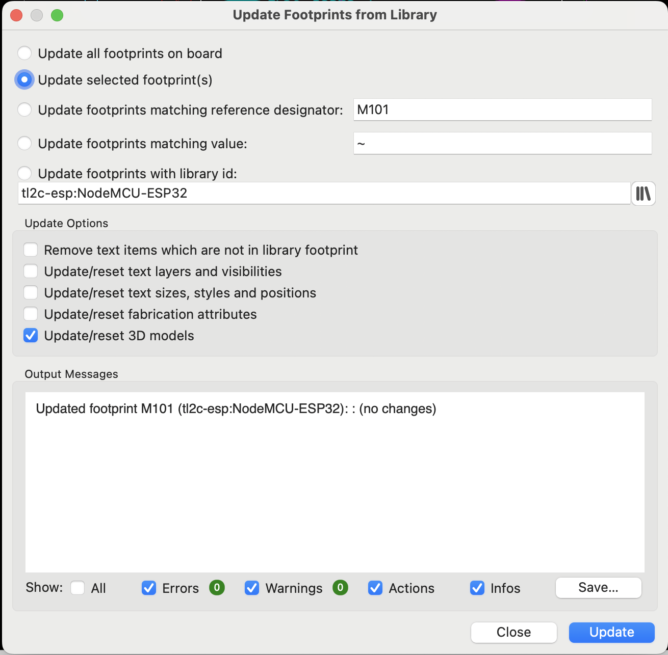
When changes are made to the footprint in the library, then the footprint needs to be updated to pick up any changes to the 3D properties in the design. I do this by using the Right-Mouse-Click on the footprint and select Update Footprint… The subsequent dialog will enable the 3D model to be updated and then you should be able to see the fully assembled board.

With these techniques I am able to quickly share and locate my parts between projects. It also means that I don’t have worry about vanishing footprints off the layout which also saves time not having to add them again.

You can save some time and just use the “Not in schematic” checkbox. https://docs.kicad.org/8.0/en/pcbnew/pcbnew.html#footprint-attributes That will prevent KiCad from removing unmatched footprints (when you ask it to during update)
LikeLiked by 1 person
Thanks. That has been around since 6 and I have not used it! The only advantage what I do is that I can manage all the footprints, in the schematic Symbol Fields Table, which I use a lot.
LikeLike