
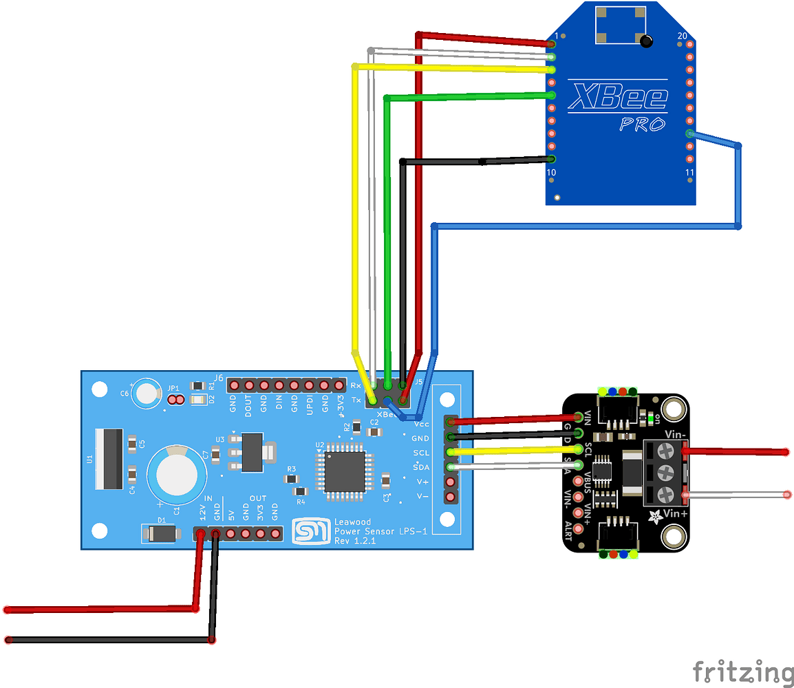
When I have the time, I like to document my boards, and part of that is producing wiring diagrams that are clear enough for someone else — or a future me — to follow without too much head-scratching. For that, I’ve always been drawn to Fritzing. There’s something about the style of a Fritzing diagram that works particularly well: the boards look almost realistic, the components are recognisable, and the whole thing has a clarity that a raw schematic doesn’t always have.
The problem comes when you want to include a custom PCB you’ve designed in KiCad. Getting it into Fritzing as a proper part isn’t impossible, but it’s a fair amount of work — you have to hand-craft the .fzp metadata file, draw the breadboard SVG, map every connector pin, and get the geometry close enough to be useful. I attempted this once for one of my own boards and decided there had to be a better way.
That got me thinking about whether the process could be automated. KiCad already has all the information Fritzing needs — the board outline, connector positions, net names, pad coordinates. The result of that thinking is PCB2Fritzing, a KiCad Action Plugin (and CLI utility) that reads a KiCad PCB layout and generates a ready-to-import Fritzing part (.fzpz) from it.
I wouldn’t call it finished, but it’s at a point where it’s genuinely useful, so I thought it was worth writing about — including the rather interesting journey of getting here.
A Learning Experience on Several Fronts
This was my first attempt at writing a plugin for KiCad, so I went in knowing it would be a learning experience. What I didn’t fully anticipate was quite how many dimensions that learning would take.
For a start, KiCad is in the middle of transitioning its plugin framework – moving from the older SWIG-based bindings to a new IPC (Inter-process Communication) approach. The plugin started out using SWIG but I soon shifted to IPC. So, in the end, I was able to get the plugin working with both SWIG and IPC, but understanding the differences between them was something I had to pick up along the way.
The other significant dimension was that I used vibe-coding to build the plugin — working iteratively with an AI to handle the heavy lifting of the actual implementation. I’ll be honest: this saved a considerable amount of time and effort. But what I found particularly interesting was that the AI wasn’t just writing code. As my understanding of the KiCad plugin framework improved, I could tune my prompts to get better results — and the AI, in turn, helped me understand the intricacies I didn’t yet know to ask about. It was genuinely a two-way process.
How the Approach Evolved
The development didn’t happen in one go. It went through three fairly distinct stages, and each one taught me something that shaped the next.
Stage 1 — Using pad information
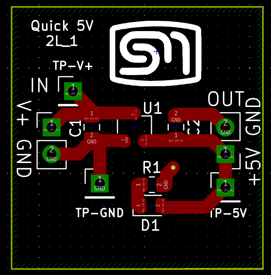
The initial approach was to extract the pad geometry directly from the KiCad board and use that to construct the Fritzing part’s SVG. This worked, after a fashion, but the results weren’t particularly satisfying. Pads give you the electrical information, but they don’t give you a very readable picture of what the board actually looks like.
Stage 2 — Using the silkscreen
The natural next step was to overlay the silkscreen layer instead. This is much closer to what you’d expect a board to look like in a wiring diagram — labels, component outlines, the kind of thing that makes a part recognisable. An improvement, certainly, but it still felt like a somewhat flat representation.
Stage 3 — Using the KiCad CLI 3D renderer
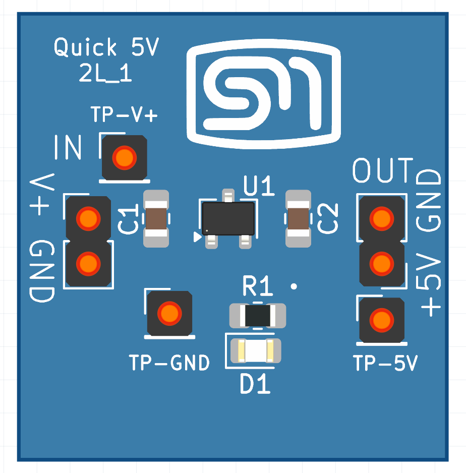
The third approach was the one I’d been working towards without quite knowing it. Rather than trying to reconstruct a representation of the board from its layers, the plugin now uses kicad-cli (KiCad Command Line Interface) to produce a full 3D render of the board and embeds that as the breadboard image in the Fritzing part. The result is a properly rendered, realistic-looking board — which is exactly what I wanted from the start.
This is now the default mode, and honestly it’s the version that made the whole project feel worthwhile. The trade-off is that the 3D render can take 30–90 seconds depending on your board’s complexity and your hardware, so if the export dialog sits quietly for a while, that’s expected — it’s waiting on kicad-cli to finish.
What It Does
At its core, the plugin extracts the relevant information from your KiCad board and assembles it into the set of files Fritzing expects:
- A
.fzppart descriptor withfamilyandtypemetadata - SVG views for breadboard, schematic, PCB, and icon
- A board outline derived from the
Edge.Cutslayer (supportinggr_rect,gr_line,gr_poly, andgr_arc) - Connector mappings for pin header footprints — the most common case for custom boards dropped into wiring diagrams
- A validation report to catch consistency issues before importing
- Everything bundled into a single
.fzpzpackage
Installing the Plugin
PCB2Fritzing is available directly from the KiCad plugin repository, so the easiest way to install it is through the Plugin and Content Manager (PCM) built into KiCad. Open PCM, search for PCB2Fritzing, and install it from there — no downloading or manual file handling needed.
If for any reason you’d rather install it manually, the latest PCB2FritzingPart-pcm.zip is available on the Releases page on GitHub. In that case, open PCM, choose Install from File, and point it at the downloaded ZIP. There’s also a full manual install guide in docs/KICAD10_EXTENSION_INSTALL.md in the repository if you need it.

Once installed, open your board in the PCB Editor. The plugin appears under Tools → External Plugins and on the toolbar. Running it opens a dialog with:
- An output directory selector
- Part Family and Part Type fields (the defaults are fine for most cases)
- A Generate button that runs the export without closing the dialog
- An output log showing what’s happening step by step
- A Save… button to write the log to a file if something goes wrong
Once it’s done, open Fritzing, go to My Parts, and import the .fzpz from your output directory.
Using the CLI
The same conversion is available from the command line if you’d rather work outside KiCad:
python3 -m venv .venv. .venv/bin/activatepip install -e srcpcb2fritzing path/to/board.kicad_pcb --out-dir build/fritzing-part
You can also override the default part name:
pcb2fritzing path/to/board.kicad_pcb --out-dir build/fritzing-part --part-name my-custom-par
Current Limitations
It’s worth being upfront about where things stand.
Connector scope: Connector extraction currently covers pin header footprints. Other types – screw terminals, SMD pads and so on — are on the to-do list but aren’t there yet.
Colour rendering in 3D mode: Pad colours in Fritzing can look slightly different from what you might expect – usually a bit brighter or more orange. This is a compositing effect from the embedded 3D imagery rather than anything wrong with the generated file.
Stale parts from earlier versions: If you’ve been experimenting since the early releases and see Fritzing startup warnings about local parts scanning, it’s worth clearing out old pcb2fritzing.* entries from the local parts folder (on macOS: ~/Library/Application Support/Fritzing/Fritzing/local_parts/user/) and re-importing the latest .fzpz.
What’s Next
The main things I’m working towards:
- Expanding connector extraction beyond pin headers
- CLI flags for
--part-familyand--part-typeto match the plugin dialog - Migrating fully to the KiCad IPC plugin framework for KiCad 11+
Give It a Try
The source is on GitHub at github.com/SteveMayze/KiCad2Fritzing. The latest release is v0.4.1. If you run into a board that doesn’t parse correctly, raising an issue with a minimal test case is the most helpful thing — it makes it much easier to track down what’s going wrong.


One thought on “Creating a Fritzing Part From a KiCad PCB”