
In this post I bring together three previous projects into a finished solar-powered wireless sensor network for the garden shed — gateway, end node, and battery monitor, talking over XBee. It’s a long one, covering the design decisions and lessons learned, plus a technique I picked up from a KiCon 2024 talk: using KiCad to lay out control panel wiring.
Motivation
The original motivation for this project came about quite a while ago when talking to a friend and his need to monitor the batteries that were charged by solar cells. Back then, when I decided to start this project, the most popular radio modems were Digi XBee modules with ZigBee. Since then LoRa and LoRa WAN have come into play, but I have been stubborn to stay with XBee. Mainly because I had made the investment and figured, if designed correctly, I should be able to replace the radio module and update the firmware to create drivers for the new module. In order to realise this project, I needed somewhere local and tangible that I would apply this to. Since our garden shed does not have any power or light, I decided that it would be a good idea to install a solar cell there with a lamp and therefore I have the perfect place to install and test this project.
The full project has suffered from scope changes and interruptions from other projects. Three such projects have been documented separately.
- Trying out the INA219
- Creating a Gateway Node using XBee and Test Driven Development
- Developing a Remote Sensor Firmware using Test Driven Development
Design
System Model
I started the conceptual design using the Unified Modelling Language (UML). I like its standardised nature, and using the right tool makes creating the model and diagrams easy. The tool I prefer to use is Enterprise Architect from Sparx Systems. The main difficulty with UML is understanding how to express the ideas one has into a tangible model that others can understand. I started with a context model. This is an abstract model of the components of the system being designed. In my case, I was calling it a Field Device which, in itself, has no meaning. It is not until we examine the other components, especially the implementation of the Sensor Module, that we see this becomes a battery health monitor. The major components are a power system, sensor module, telemetry unit and MCU module. I did not add the I2C temperature sensor as I considered this to be an optional extra and I did not want to shift focus from the main purpose of the sensor – voltage and current.

SinceI fleshed out this design with an Internal Block Diagram (ibd). This type of diagram is a great place to think about and define the specifications of the power requirements and how the MCU will communicate with the other modules i.e. the telemetry unit and the voltage/current sensor.

Communication Protocol
I had several attempts at creating the battery health monitor, largely based on the Trying out the INA219 project. I was never satisfied with these as they are all bound to my lab bench and breadboard. I needed some concrete installation that would prove the concept of what I was trying to build. I therefore stepped back and thought about how the data collected would be used. I then realised a type of gateway would be useful: a device to collect the data from the end node sensor and post this to a database where I could see and use the data. I then set to work on Creating a Gateway Node using XBee and Test Driven Development. Here with the help of a wonderful reference book, Test Driven Development with Python (Percival, Harry J.W. Test Driven Development with Python – Obey the Testing Goat: Using Django, Selenium & Javascript. 2nd Ed., O’Reilly, 2017), I could use Test Driven Development (TDD) to create a Python application that would listen for broadcast messages received by an XBee and, using a protocol, request information from the end node devices. For this to work effectively, I needed a protocol. The main requirements for the protocol are that:
- Be asynchronous
- Be self-learning
- Be simple
The basic premise of the asynchronous nature of the protocol is that the end node device i.e. the sensors, are autonomous in that they are not listening for commands from the gateway node, but rather, they announce their presence with a READY message. The gateway will then validate their address with a register. If they are not registered, they will be treated as a new device and the gateway will respond with a NODEINTROREQ message (node introduction request). This will trigger the end node to introduce itself to the gateway. This was where the protocol got interesting with respect to the second requirement – self-learning. This got me thinking about how to enable the gateway to accept new devices without having to dictate/hard code the device configuration i.e. the data expected etc. Going back to the abstract nature of the block diagram, I came to realise that the gateway could be dealing with at least two types of devices – Sensors or Actuators. Sensors will be expected to send information whereas actuators can be expected to receive some type of command (on/off, open/close), though an actuator could also be expected to report its current state. Within these categories or Class of sensor as I refer to it, there is still another categorisation that I call Domain. For these devices, the domain could be Power, Rate, Capacity or Infra, to name a possible few. For each combination of these classes and domains, there will be a set of values that can be expected to be received from the device. Some of the values I have come up with are shown in the following table.
| DEF_NAME | UNIT | MULTIPLIER | DESCRIPTION | SYMBOL | LABEL | CLASS | DOMAIN | TOKEN |
|---|---|---|---|---|---|---|---|---|
| Liquid Flow | litres per second | 1 | The rate of flow for a liquid | l/s | liquid_flow | SENSOR | RATE | 53 |
| Bus Voltage | Volts | 1 | The supply voltage to the system | V | bus_voltage | SENSOR | POWER | 49 |
| Load Current | milli Amperes | 1000 | The current being drawn by the load | mA | load_current | SENSOR | POWER | 51 |
| Core Temperature | Celsius | 1 | The internal temperature of the sensor processor | C | core_temp | SENSOR | INFRA | 52 |
| Water level | Percent | 1 | The water level | % | water_level | SENSOR | CAPACITY | 54 |
| Shunt Voltage | milli Volts | 1000 | The sense voltage | mV | shunt_voltage | SENSOR | POWER | 50 |
Tokenisation
One restriction I discovered when working with XBee is the frame-size of 73 bytes for XBee DigiMesh. This means that data formats such as JSON are out of the question. I then came up with a tokenising scheme so that the elements of the data to be sent would be tokenised. The downside of this approach is that I had to define a list of values and their tokens that had to be available to both the end node and the gateway. However, the implementation of each node can decide which of those values it will send and this is the information that will be transmitted by the end node on a NODEINTRO message (node introduction – i.e. the class, domain of the sensor plus the expected data values when it sends a DATA message).
#define HEADER_GROUP 0x10
#define OPERATION_GROUP 0x20
#define PROPERTY_GROUP 0x30
#define METADATA_DOMAIN_GROUP  0x40
#define METADATA_CLASS_GROUP  0x50
typedef enum token_e {
        NODE_TOKEN_VOID = 0x00,

        NODE_TOKEN_HEADER_OPERATION = HEADER_GROUP | 0x01,
        NODE_TOKEN_HEADER_SERIAL_ID = HEADER_GROUP | 0x02,
        NODE_TOKEN_HEADER_DOMAIN = HEADER_GROUP | 0x03,
        NODE_TOKEN_HEADER_CLASS = HEADER_GROUP | 0x04,

        // OPERATIONS
        NODE_TOKEN_READY = OPERATION_GROUP | 0x01,
        NODE_TOKEN_DATAREQ = OPERATION_GROUP | 0x02,
        NODE_TOKEN_DATA = OPERATION_GROUP | 0x03,
        NODE_TOKEN_DATAACK = OPERATION_GROUP | 0x04,
        NODE_TOKEN_NODEINTROREQ = OPERATION_GROUP | 0x05,
        NODE_TOKEN_NODEINTRO = OPERATION_GROUP | 0x06,
        NODE_TOKEN_NODEINTROACK = OPERATION_GROUP | 0x07,

        NODE_TOKEN_PROPERTY = PROPERTY_GROUP|0x00,
        NODE_TOKEN_PROPERTY_BUS_VOLTAGE = PROPERTY_GROUP | 0x01,
        NODE_TOKEN_PROPERTY_SHUNT_VOLTAGE = PROPERTY_GROUP | 0x02,
        NODE_TOKEN_PROPERTY_LOAD_CURRENT = PROPERTY_GROUP | 0x03,

        NODE_TOKEN_PROPERTY_TEMPERATURE = PROPERTY_GROUP | 0x04,
        NODE_TOKEN_PROPERTY_FLOW = PROPERTY_GROUP | 0x05,
        NODE_TOKEN_PROPERTY_LEVEL = PROPERTY_GROUP | 0x06,

        // METADATA
        NODE_METADATA_DOMAIN_POWER =  METADATA_DOMAIN_GROUP | 0x01,
        NODE_METADATA_DOMAIN_CAPACITY =  METADATA_DOMAIN_GROUP | 0x02,
        NODE_METADATA_DOMAIN_RATE =  METADATA_DOMAIN_GROUP | 0x03,
        NODE_METADATA_DOMAIN_INFRA =  METADATA_DOMAIN_GROUP | 0x04,
        NODE_METADATA_DOMAIN_ALL =  METADATA_DOMAIN_GROUP | 0x0F,

        NODE_METADATA_CLASS_SENSOR =  METADATA_CLASS_GROUP | 0x01,
        NODE_METADATA_CLASS_ACTUATOR =  METADATA_CLASS_GROUP | 0x02,
        NODE_METADATA_CLASS_ALL =  METADATA_CLASS_GROUP | 0x0F,
    } Token_t;
Once registered, the end node will keep track of the gateway node and will only communicate with that node from then on. Once the gateway has recorded the sensor details, the next time the end node sends a READY message, the gateway will respond with a DATAREQ (request data) message. The node will then read the sensors, package the data and send this to the gateway that will then unpack the data and post this information to the database.
This description is necessarily brief. The full communication between the nodes is shown in the following state and timing diagrams. Here the various states of the node and gateway are shown, along with the communication stage each is at. Note that the gateway will respond to the end node with an acknowledgement that its information has been received OK.

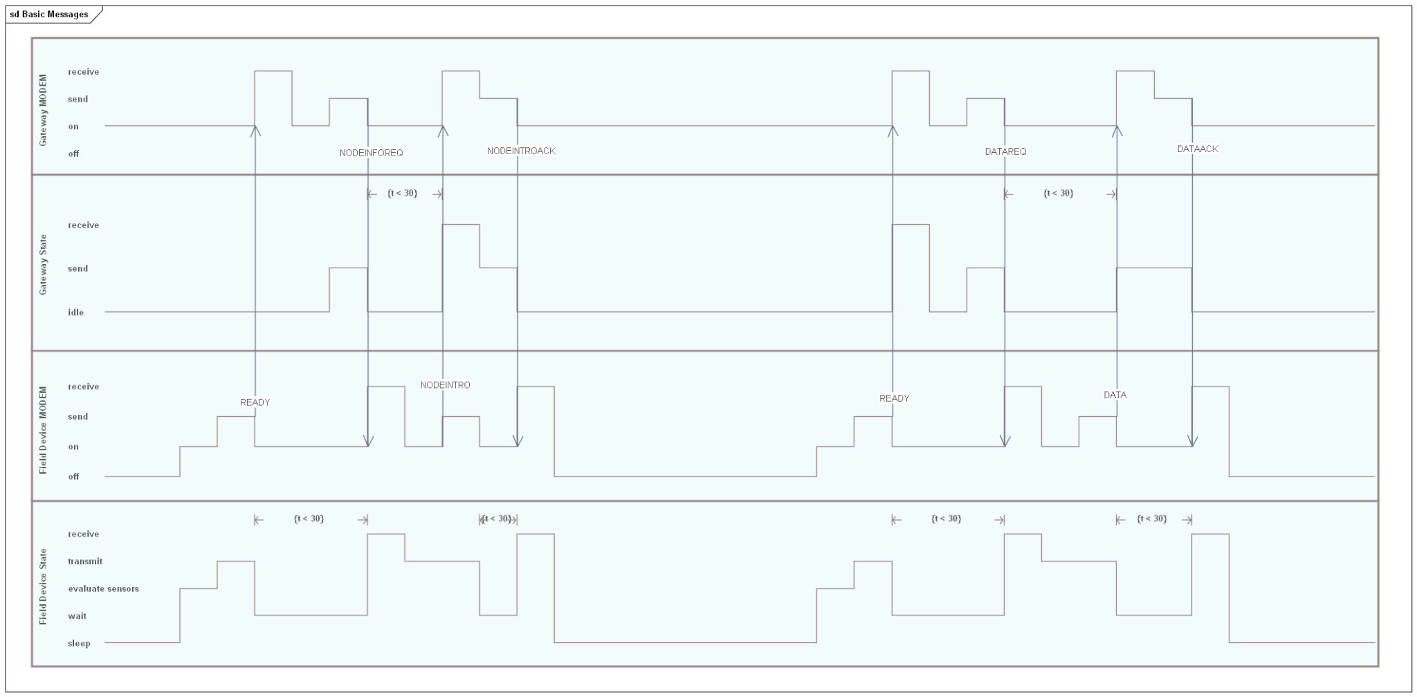
The advantage of this approach is that I don’t need to preregister the sensors. The idea is that they will register themselves but the registration is based on a set of pre-seeded assumptions about the class and domain of the sensor and the expected data that will be received by the sensor. Another advantage of this approach is that, now I have a formal protocol, creating the actual end node was easier: I have a defined API I needed to implement against and I also now have the means to formally test it.
Implementation
Board and MCU
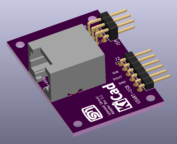
Since getting back into electronics, I have joked that the hardest part is the mechanical design. I find this is an area where a lot of decisions need to be made that can affect the size and shape of the PCB, and with the sensor, there was no exception. The size and shape of potential enclosures are innumerable. I settled for one that I had picked up at a trade fair for no good reason other than it looked good and seemed to be the right size. So I had to make it work. The first thing was the board, and therefore I had to select an MCU to do the job. It had to have the minimum of an I2C port and at least 2 USART ports. One would be dedicated to communicating with the XBee, the other used for logging. I am familiar with the Atmel/AVR range of chips and find them simple to work with. I decided on the ATMega1608. Thinking about the board design, I thought it would be a good idea to have the INA219 (Adafruit) board plug straight into it. I also needed provision for programming and to connect a USB/USART adapter. I had experimented with adding a USB/USART chip to the board, but couldn’t get it working properly. I also felt it would be an expensive option only needed during development and troubleshooting, so instead I exposed the second USART and used an off-the-shelf USART/USB adapter. This then got me thinking about the enclosure. How would I bring this all together so that it was robust and usable? I then got the idea of an IP65 RJ45 connector. They are robust and have 8 pins available. Just enough to expose the Unified Program and Debug Interface (UPDI) and USART. I found one called the etherCON from NEUTRIK (part number NE8FDIS-TOP) that suited my requirements perfectly. The etherCON module has a 2.54mm pitch 2×3 pin header connector at the rear, so I could use a standard 2×3 pin ribbon cable connector to connect this adapter to the PCB.


To help with future testing, I broke away from the main project and started an interim and quick project to create an adapter board. The purpose of this board would be to take the RJ45 cable that is connected to the sensor module and break this out so that the ISP and the USART/USB adapter can be connected.
Power System
With respect to the power system – I opted to use Low Drop Out (LDO) regulators to go from 12V to 5V and then from 5V to 3.3V. I understand that switching power regulators would be much more efficient, but I had the LDOs in stock and I considered it would be more work to introduce a switching power supply when my focus lay elsewhere in this project.
Enclosure
I still had the problem of the board size. The enclosure is slotted to allow boards to slide in. As a hobbyist, a board of this size would be expensive and unnecessary for the number of components I need to use. I therefore opted to keep the board design small with mounting holes and mounted the board to a sheet of plastic that could be inserted into the enclosure. This then gave me space to also install a separate XBee breakout board. I came up with the 66mm x 30mm PCB, flanked on three sides by pin headers for the RJ45, XBee, INA219 board and the power input and output.
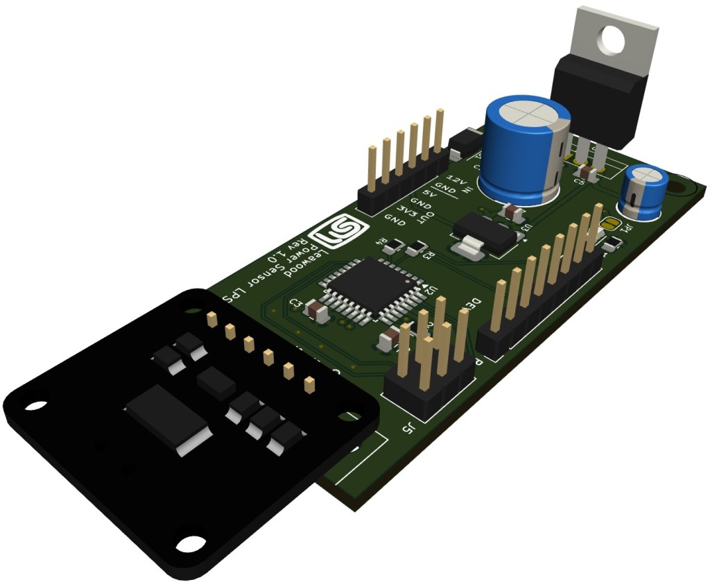
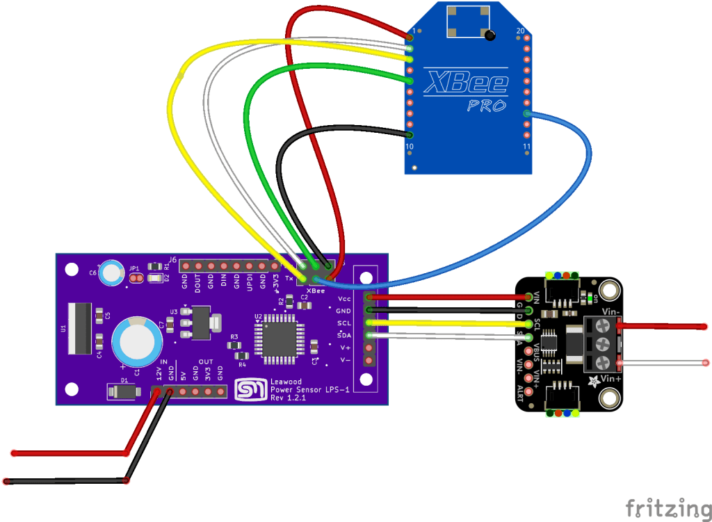
The next stage was to bring this all together into the chosen enclosure. Using Inkscape, I created the mask for making the holes to take the antenna, three connectors (I later had to modify this to add an additional connector) and the RJ45 connector. Before drilling the front panel, I attached the mask to some stiff board, cut this out and installed this into the enclosure to verify the spacing of the components. Once satisfied, I could then drill and cut the holes.

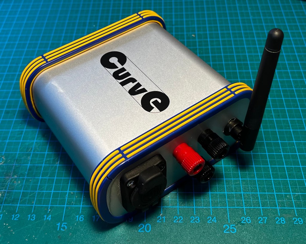

I was now all set. I had a gateway that I could test against, and I had a means by which I could program the device and monitor any logging from the device – Note that the UPDI interface for the AVR devices has rudimentary debugging capabilities but I find using it is rather cumbersome in the MPLAB X IDE – or I don’t have the right experience to use it properly. One thing on my list of things to do (i.e. learn) is to use JTAG one day, but not now. I find the most effective way is to use a combination of the UPDI debugging and simple diagnostic logs. This then sparked the final project in the suite – Developing a Remote Sensor Firmware using Test Driven Development. I always liked the concept of test driven development but had no idea as to how to apply this to firmware development. I studied the documentation for Unity and CMock as referenced in Test-Driven Development for Embedded C (James W. Test-Driven Development for Embedded C. Pragmatic Bookshelf, 2011). That, in conjunction with the method proposed in Test Driven Development with Python, let me use the MPLAB X IDE to develop the firmware with tests running against the ATMega1608 simulator. I found this a very rewarding experience as I had no reliance on any hardware during this process. Once I had the board available, I could then apply the firmware which largely worked out of the box. There was some tweaking to do but I found this process quite productive.
Installation
The final stage was the installation of the system as a practical example. I chose our garden tool shed. This has no power and therefore no light. Any battery-operated lamp I have installed never worked as the batteries were always flat by the time I got to use it. I now needed to procure and install a solar panel, battery and charger. I opted to get an off-the-shelf charger rather than creating my own since the focus of this project was the sensor. For this installation I didn’t need anything high-powered, so I opted for a 10W solar panel and a 7.2Ah sealed lead-acid battery, as I wanted to keep things small. I had some other constraints for this project:
- The charging system and load devices need to be protected by suitable fuses.
- I should be able to isolate the battery from the system.
- I should be able to switch the sensor out of the system so that the battery and charger work in isolation.
- I wanted to be able to wire up the panel, install it such that I would only have to connect the solar panel and the cable for the lamp on site.
- The system should be enclosed in a self-contained enclosure – preferably IP65.
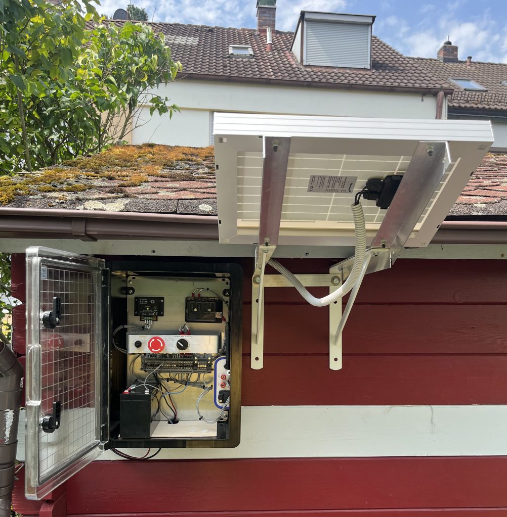
I eventually found a cabinet small enough (Boxexpert BXPPABSBT300400170-F01) to suit my purpose. The problem I had was how to wire this up so that it looked reasonable. The presentation CE for Makers by Clemens Mayer at the 2024 KiCon conference gave me the idea to use KiCad as a wiring tool. Here I could use the schematic tool to model the connection between the various components and realise the switch connections to implement the battery kill switch and direct/monitor modes. In the PCB layout, I created a 1:1 model of the cabinet with 1:1 footprints of the devices to install – the charger, battery, battery monitor, fuse box and switches. This proved very effective for visualising the positioning of the items before drilling the back panel.
It was during this stage that I realised that there was a shortcoming in my initial assumption for the monitor. I had installed only three terminals – 12V+ IN, GND and then LOAD. This implies that the sensor unit will be powered by the same bus that will be monitored. I realised that a more interesting metric would be the charge current. I therefore had to drill an extra hole in the enclosure and add a new connector so that I now have 12V+in, GND, Vin+ and Vout+. This allows me to power the sensor as part of the load on the battery, but the bus to be monitored would be that from the charging unit to the battery i.e. the charge current.
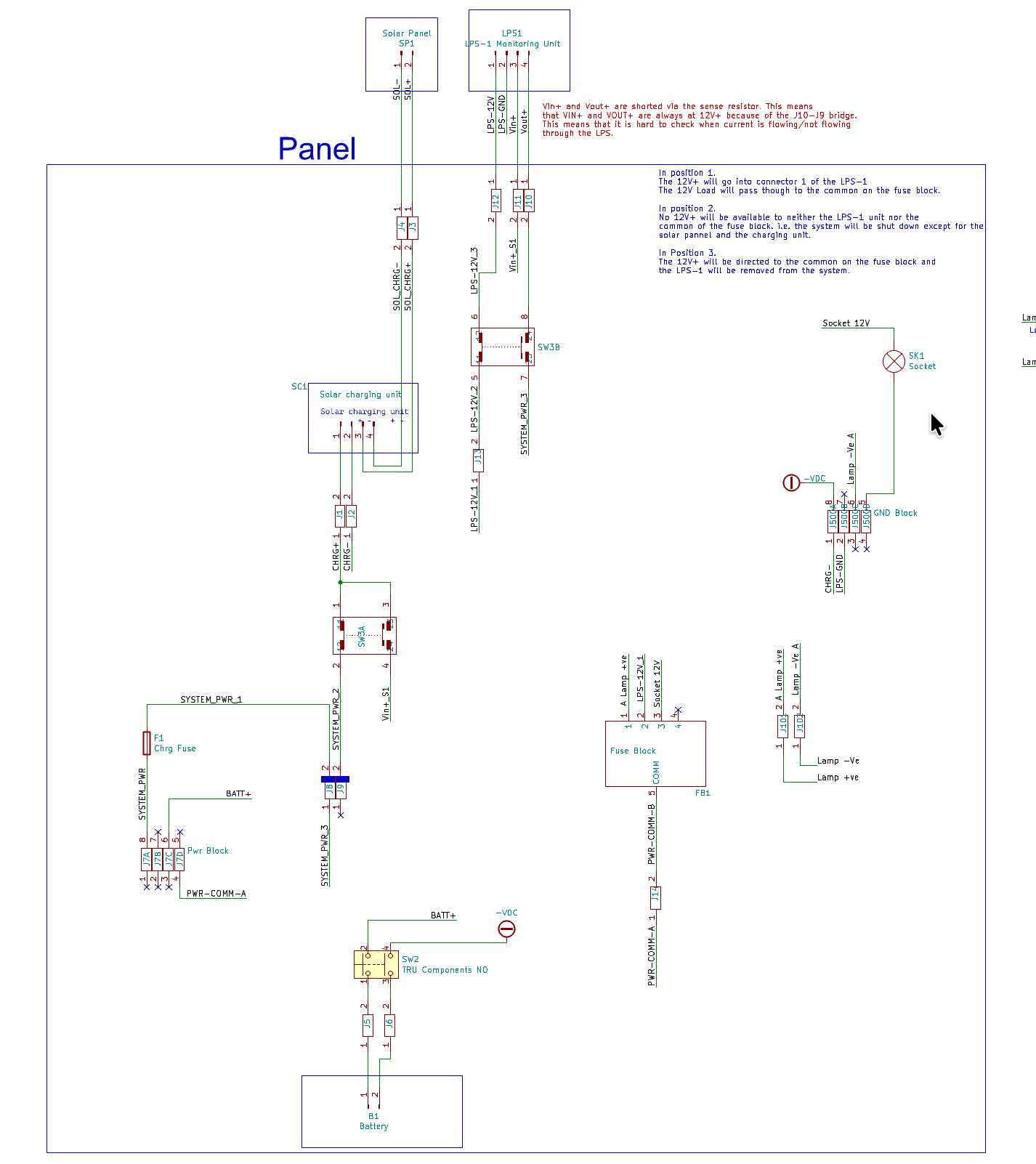
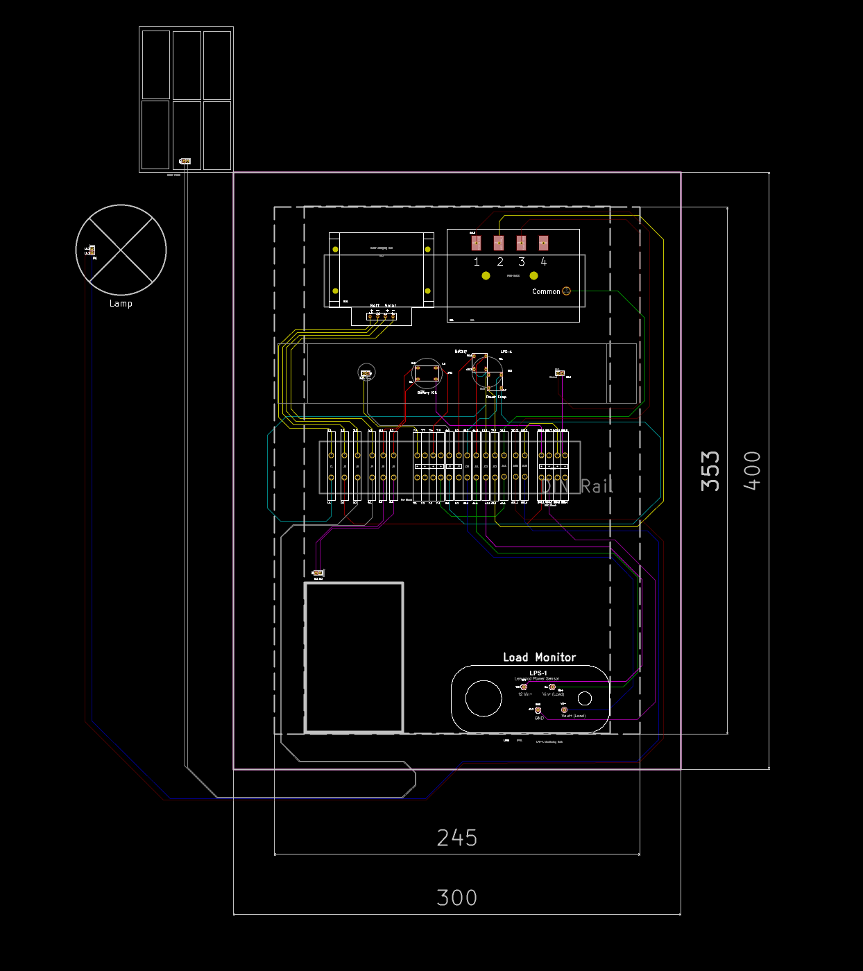
With the wiring of the system worked out, I could then finalise the type of switches to procure and fit everything into the cabinet. Constructing the panel in this way meant that I could assemble and test the system in my workshop, and the installation on site was an easy connection of four conductors.
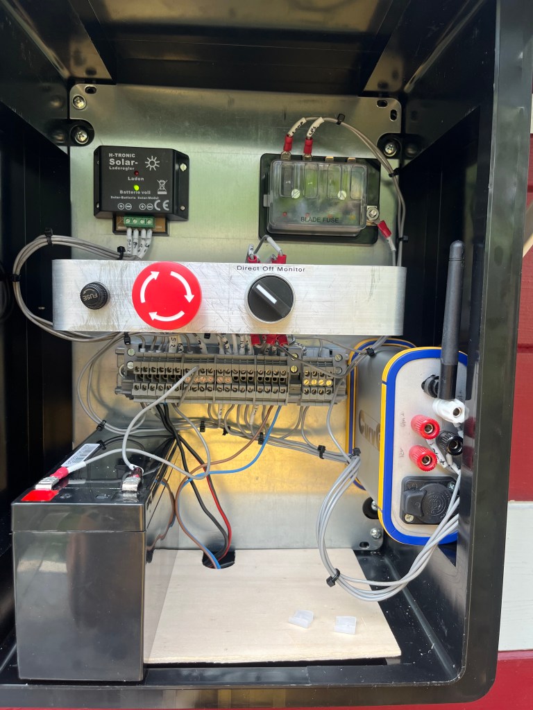
Conclusion
Once installed, I started up the gateway and checked the database. The data is coming through with no issues. So this project as a proof of concept is complete, but the work does not stop here. I am not satisfied with the power required to drive the sensor. With its current configuration, the sensor will draw 9mA when idle and then up to 43mA when communicating with the gateway. The idle current draw is way too high, so there are a few things I could consider doing:
- Reduce the sample rate of the end node. For development purposes, it will communicate with the gateway every 30 seconds. This could be reduced to once every hour once everything has been bedded down.
- Use switching power regulators instead of Low Dropout Regulators.
- Use a FET or similar to control power to the INA219 to switch this off during idle time.
Aside from the power budget, there are some additional features and directions that would be interesting to pursue:
- While defining the wiring of the cabinet, I came to realise that monitoring the charging current would be a more interesting metric than the load current. There is an opportunity to reconfigure the device to support more than one INA219 module so that each module could be placed on the charge line and the load line. The data message format may have to be revisited to enable this support.
- I mentioned that I stayed with XBee because I had some modules available, and LoRa came in after I had started. I now have all the infrastructure in place, so moving towards LoRa-based communication seems like a reasonable move forward.
Overall, I am very satisfied with the outcome of this project. We now have a reliably working lamp in the garden shed, the battery is staying charged, and I can see data being posted to the cloud. The power budget gives me a task for a future post.
 Rebooting Electronics
Thanks for writing this up Steve. Do you have any thoughts on where the 9mA is going, as proportions? Are you setting the INA219 and radio into their low power modes?
LikeLike
Thanks @smerrett79, I do put the radio to sleep and that made a huge difference (around 30mA). Honestly, I had not been putting the INA219 in power-down mode. I ran a quick check on my bench and putting the INA219 reduced the consumption by 4mA which is a lot more than what the data sheet gives for the Quiescent current of the device. There is still 5mA to account. The only thing I can think of is the chaining of LDO regulators. I will need to research further.
LikeLike
Good work! From a quick look at the Adafruit INA219 breakout, it has two 10 kOhm pullups from VDD to SDA and SCL, which may leak some current depending on the impedance of those pins, which may change during sleep. Re-routing them to a spare GPIO on the ATMEGA would be one way to selectively pull the bus lines up only when wanted. Also, a small power on indicator LED seems to be present with another 10 kOhm current-limiting resistor. Likely small but possibly worth chasing as your quiescent current gets smaller.
What regulators are you using?
LikeLike
Great questions. Rather than modifying the INA219 to check this out, I connected the module with jumper cables and disconnected the Vdd when the system should be sleeping. This had no significant effect. I also did the same with the XBee module and also no effect.
What became apparent is the 5mA is in the range that the MCU draws when idle but active i.e. not sleeping. I can’t prove that this is the case as it is behaving (functionally) as if it is sleeping. The regulators I am using are an L7805 to go from 12V to 5V and then a TC1262 to go from 5V to 3.3V.
Since I expose the 5V rail and 3.3V rail incase they are needed for some other purpose, I injected 5V after the L7805 and then 3.3V after the TC1262. There was a small reduction in the usage but again nothing significant. Your questions have encouraged me to keep investigating this. I will probably follow up with a write up on the CE build log.
LikeLike
One way to test if you are achieving standby mode might be to set up a peripheral like TCB0, which by default disables in standby, and using it to toggle a spare pin (can use CCL or EVSYS to broaden the range of outputs available). If the toggling stops when the CPU is supposed to be in standby, great. If not, that might evidence your hypothesis.
LikeLike
It is achieving standby. I configured the TCB0 as you suggested and I can see that the signal from toggling a pin stops during the sleep phase. I assembled a new PCB but only populated the power circuits. I believe now that this is the issue – i.e. the L7805. The quiescent current on this device is quite high. I should have looked that datasheet first!
The main reason I used this part was that I had it in stock. Still keeping with what I have on hand, I put a LM2931 on a SOIC breakout that I have, removed the L7805 (on the power system only board), and wired the LM2931 in its place. The reduction was as expected – This configuration is now drawing around 712μA. So the next revision of this board will contain an upgrade to the power system.
Thanks for your guidance.
LikeLike
Congratulations – that’s great reduction!
LikeLiked by 1 person